Schematics
Circuit schematics for each RS-UV3 hardware revision and the RS-UVPA power amplifier. Each schematic is two pages — the main transceiver circuit and the power/filtering section.
RS-UV3 Rev C
Section titled “RS-UV3 Rev C”First revision with LED indicators and sub-receiver RF output header (S_RX).
Page 1 — Main Circuit
Section titled “Page 1 — Main Circuit”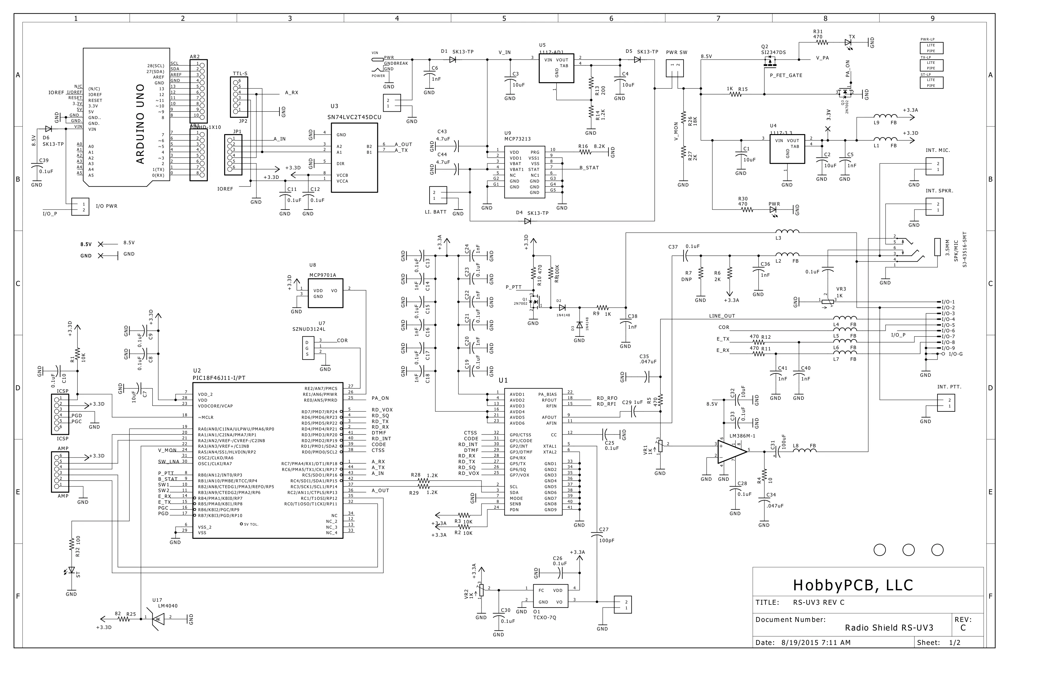
Page 2 — Power & Charging
Section titled “Page 2 — Power & Charging”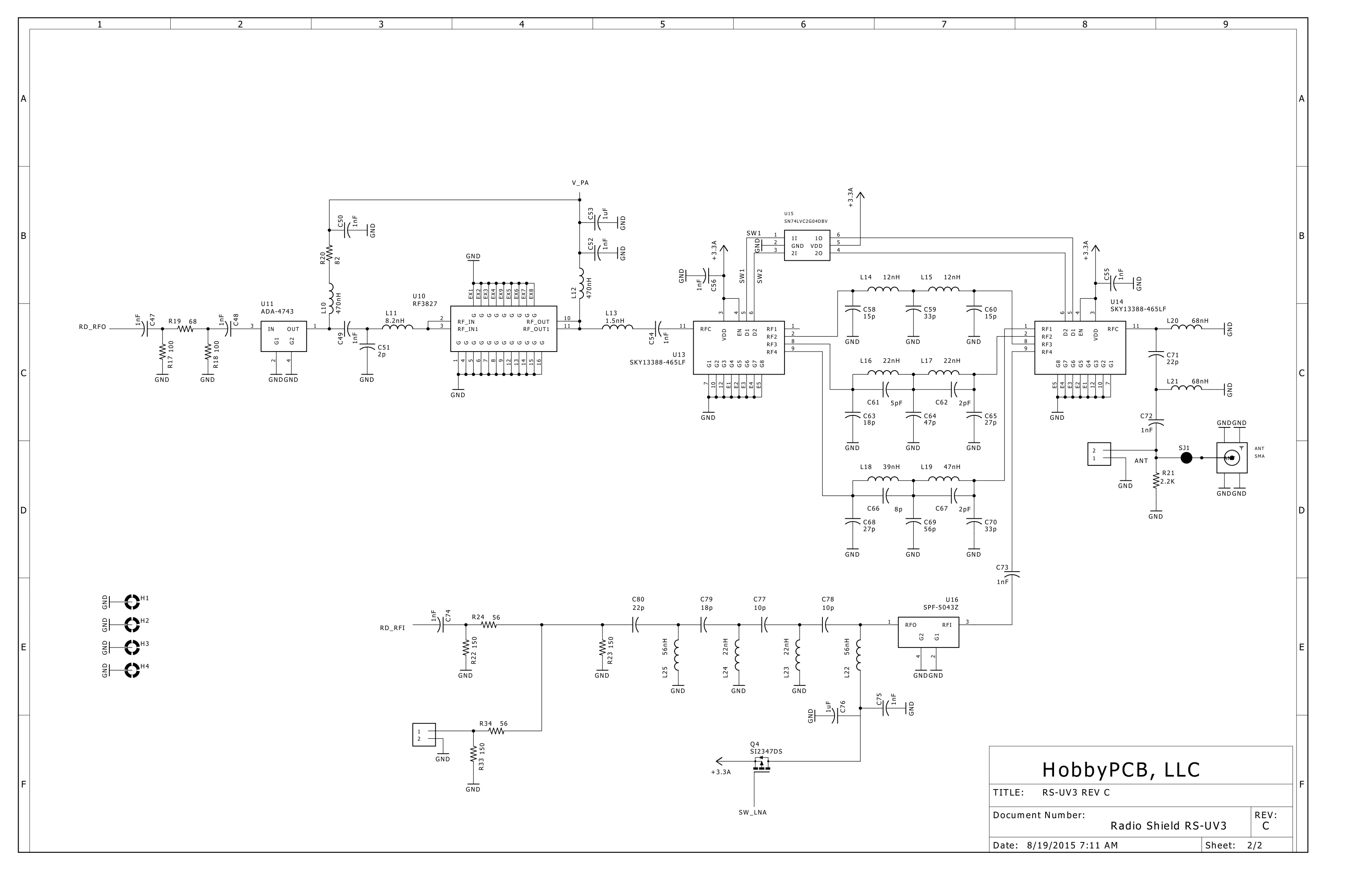
RS-UV3 Rev D
Section titled “RS-UV3 Rev D”Includes battery charge management (MCP73213), 8.4V dual-cell LiPo support, and external FTDI serial.
Page 1 — Main Circuit
Section titled “Page 1 — Main Circuit”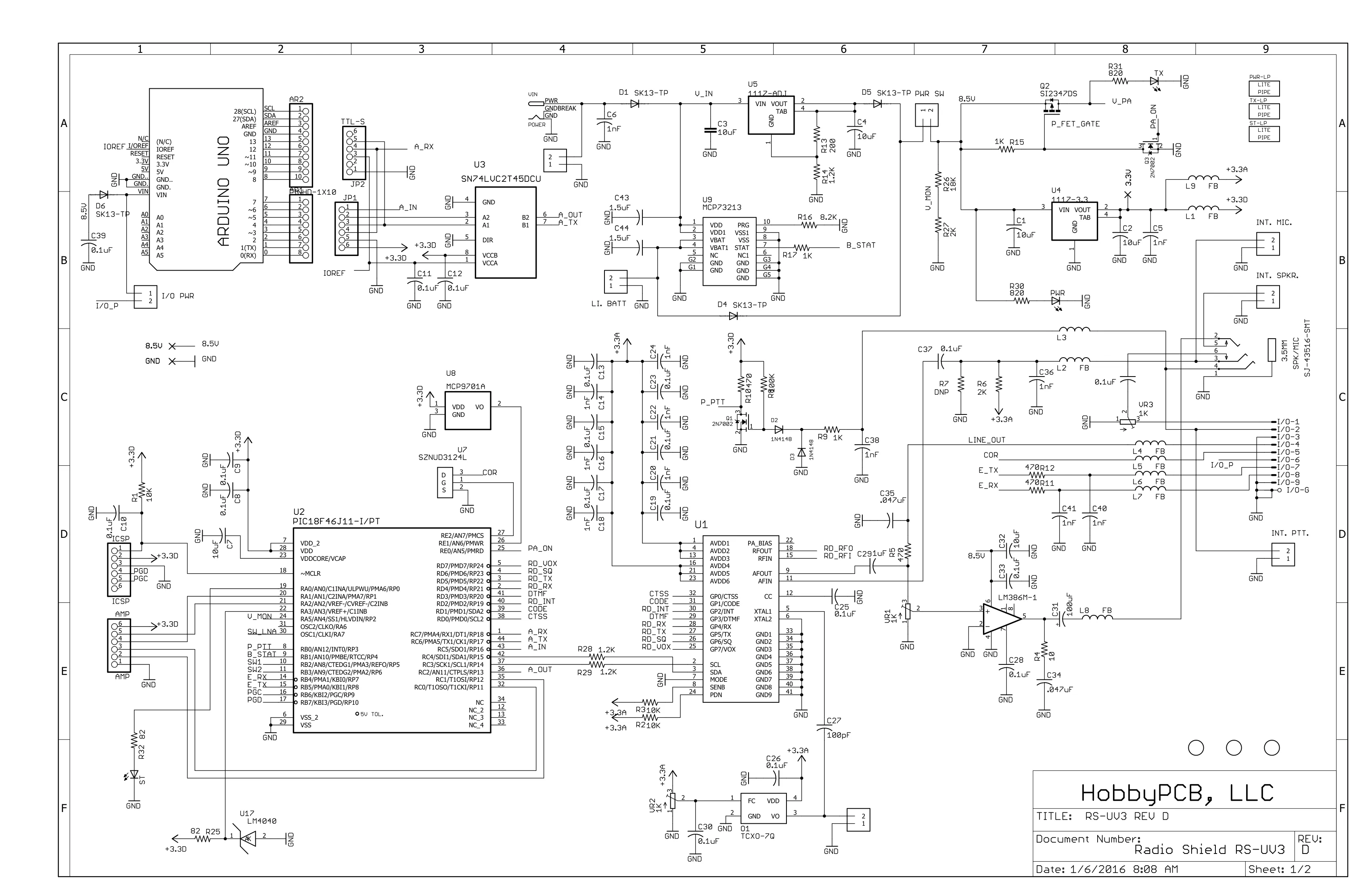
Page 2 — Power & Charging
Section titled “Page 2 — Power & Charging”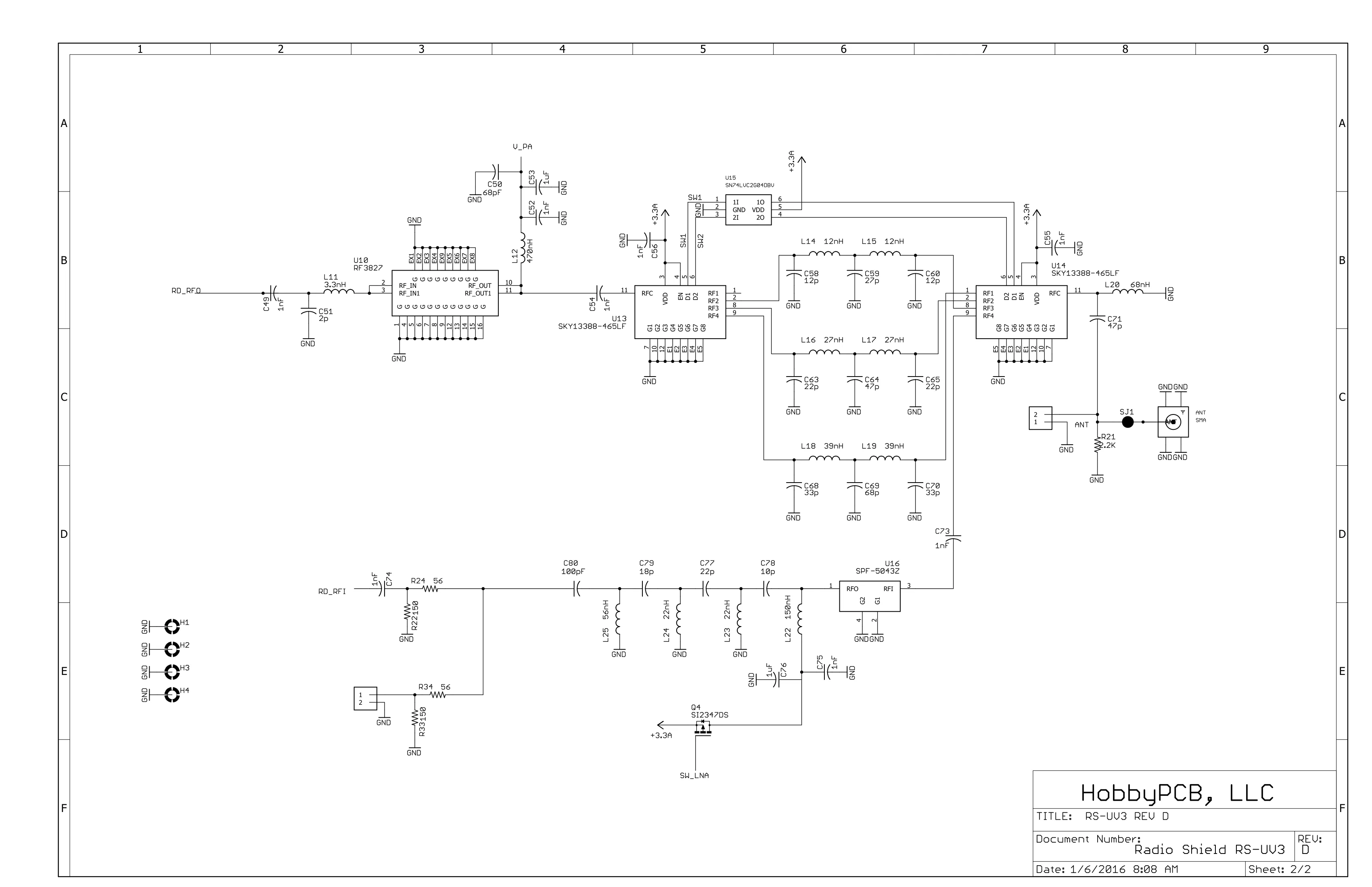
RS-UV3A Rev A (Current)
Section titled “RS-UV3A Rev A (Current)”The latest revision featuring on-board USB, buck-boost DC-DC converter, and 3.5V–16V input range.
Page 1 — Main Circuit
Section titled “Page 1 — Main Circuit”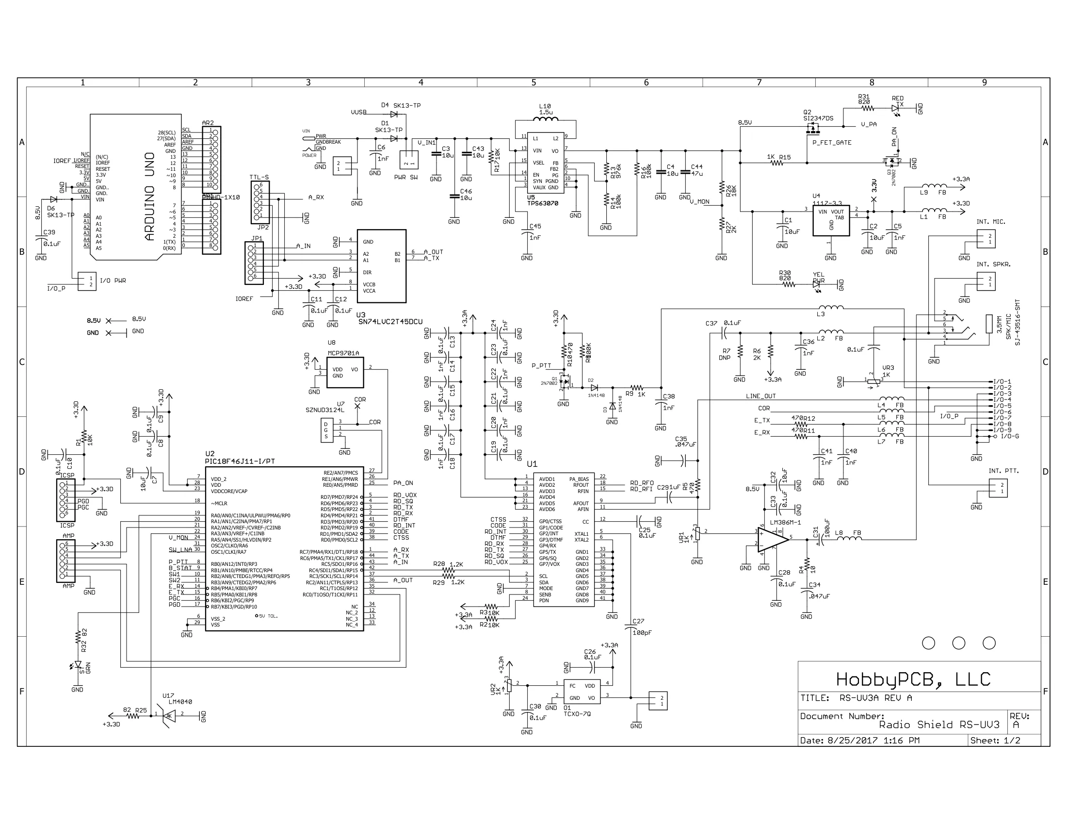
Page 2 — Power & Filtering
Section titled “Page 2 — Power & Filtering”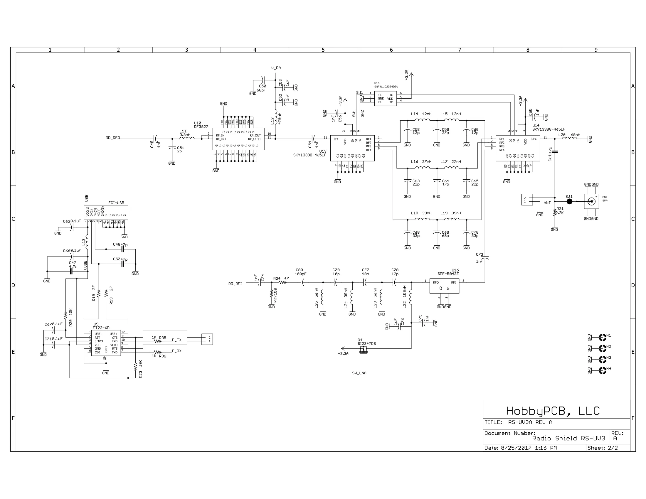
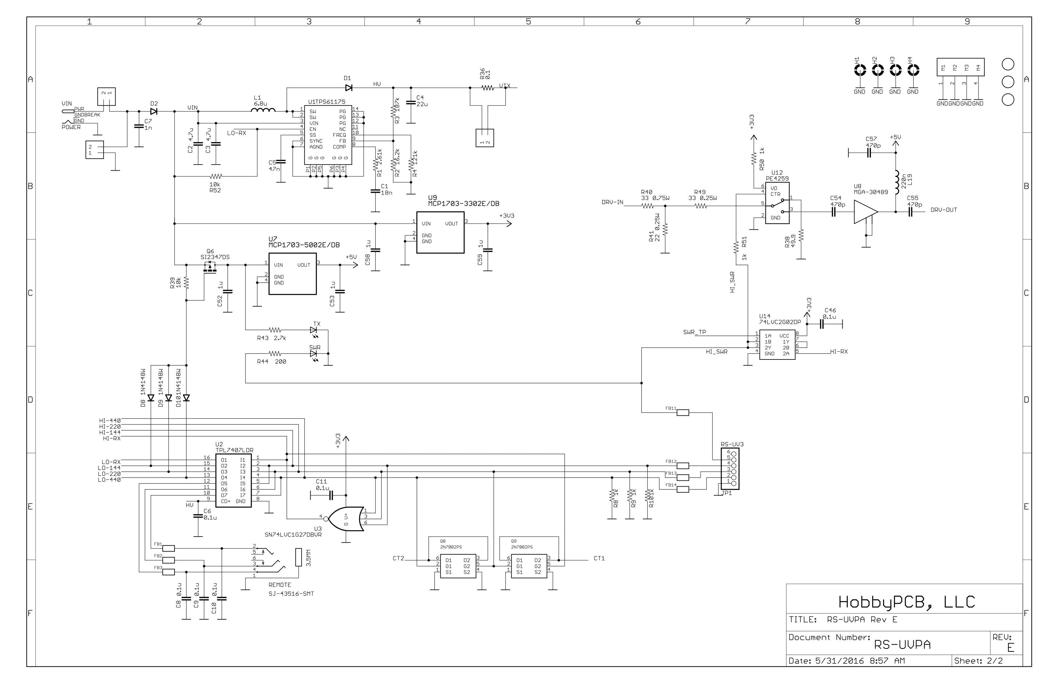
RS-UVPA Rev E — Power Amplifier
Section titled “RS-UVPA Rev E — Power Amplifier”5W power amplifier companion board with LNA preamplifier and SWR protection.
Page 1 — Amplifier Circuit
Section titled “Page 1 — Amplifier Circuit”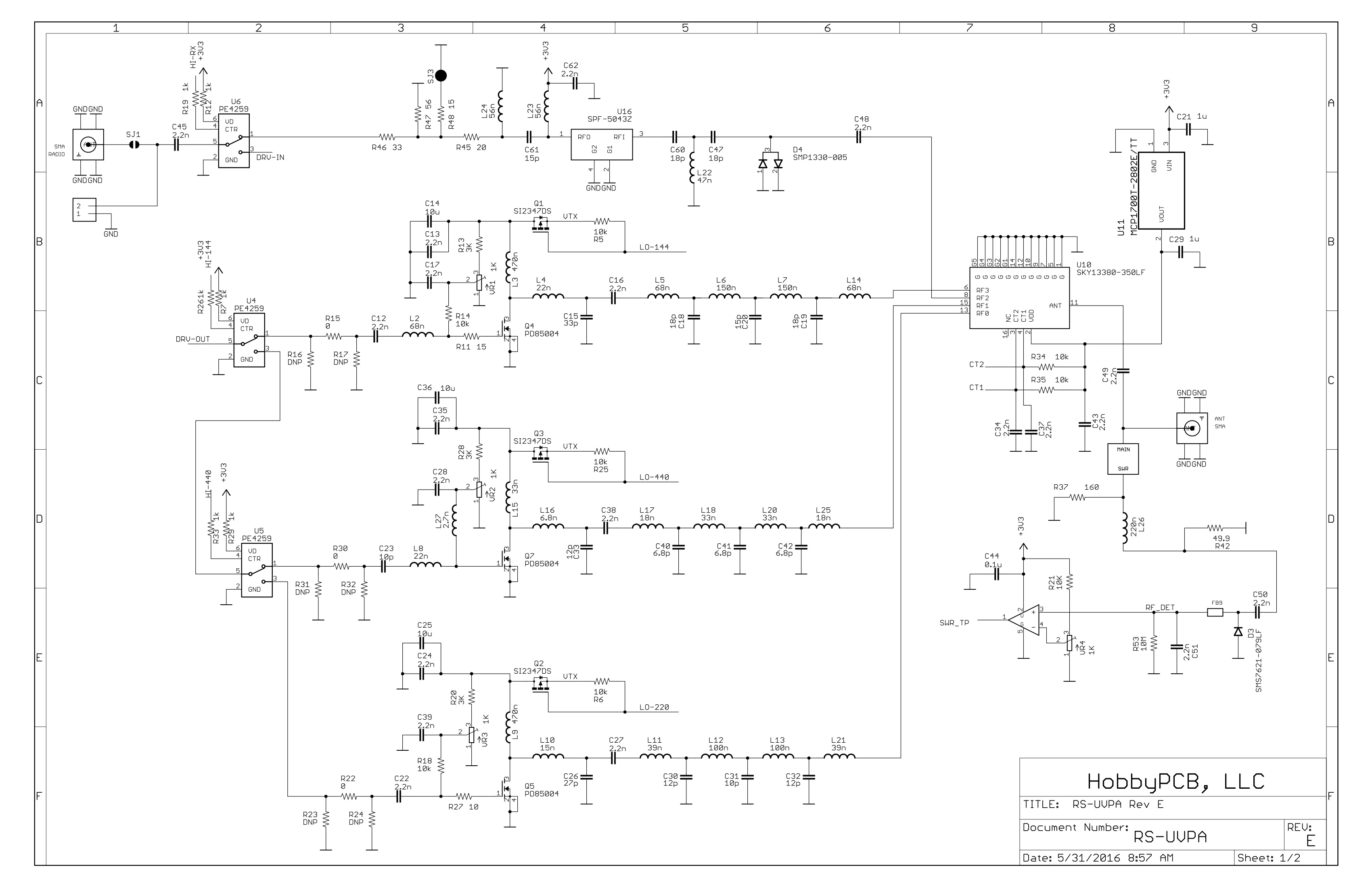
Page 2 — Filtering & Control
Section titled “Page 2 — Filtering & Control”